4002 Hardware Characteristics
Absolute Maximum Ratings
Ambient Temperature Under Bias |
0 o C to +70 o C |
Storage Temperature |
-55 o C to +125 o C |
Input Voltage and Supply Voltage |
+0.5 to -20 V |
Power Dissipation |
1.0 W |
Note that stresses above those listed in “Absolute Maximum Ratings” may cause permanent damage to the device. This is a stress rating only and functional operation of the device at these or any other conditions above those indicated in the operational sections of this specification is not implied.
D.C. and Operating Characteristics
\(T_{A}\) = \(0^{o}\) C to \(70^{o}\) C
\(V_{SS}\) - \(D_{DD}\) = 15V ± 5%
\(t_{\phi PW}\) = \(t_{\phi D1}\) = 400nsec
logic “0” is defined as the more positive voltage (\(V_{IH}\), \(V_{OH}\))
logic “1” is defined as the more negative voltage (\(V_{IL}\), \(V_{OL}\)); unless otherwise specified.
SUPPLY Current
Symbol |
Parameter |
Min |
Limit Typical |
Max |
Unit |
Test Conditions |
|---|---|---|---|---|---|---|
\(I_{DD}\) |
Average Supply Current |
17 |
33 |
mA |
\(T_{A}\) = \(25^{o}\) C |
|
Input Characteristics |
||||||
\(I_{LI}\) |
Input Leakage Current |
10 |
\({\mu}A\) |
\(V_{IL}\) - \(V_{DD}\) |
||
\(V_{IH}\) |
Input High Voltage (except clocks) |
\(V_{SS}\) -1.5 |
\(V_{SS}\) +0.3 |
V |
||
\(V_{IL}\) |
Input Low Voltage (except clocks) |
\(V_{DD}\) |
\(V_{SS}\) -5.5 |
V |
||
\(V_{IHC}\) |
Input High Voltage Clocks |
\(V_{SS}\) -1.5 |
\(V_{SS}\) +0.3 |
V |
||
\(V_{ILC}\) |
Input Low Voltage Clocks |
\(V_{DD}\) |
\(V_{SS}\) -13.4 |
V |
||
Output Characteristics - All outputs except I/O Pins |
||||||
\(I_{LO}\) |
Data Bus Output Leakage Current |
10 |
\({\mu}A\) |
\(V_{OUT}\) = -12V |
||
\(V_{OH}\) |
Output High Voltage |
\(V_{SS}\)-0.5V |
\(V_{SS}\) |
V |
Capacitive Load |
|
\(I_{OL}\) |
Data Lines Sinking Current |
8 |
15 |
mA |
\(V_{OUT}\) = \(V_{SS}\) |
|
\(V_{OL}\) |
Output Low Voltage, Data Bus, CM, Sync |
\(V_{SS}\)-12 |
\(V_{SS}\)-6.5 |
V |
\(I_{OL}\) = 0.5mA |
|
\(R_{OH}\) |
Output Resistance, Data Line 0 Level |
150 |
250 |
\({\Omega}\) |
\(V_{OUT}\) = \(V_{SS}\) - 0.5V |
|
I/O Output Characteristics |
||||||
\(V_{OH}\) |
Output High Voltage |
\(V_{SS}\) -1.5V |
V |
\(I_{OUT}\) = 0 |
||
\(R_{OH}\) |
I/O Output “0” Resistance |
1.2 |
2 |
\(k{\Omega}\) |
\(V_{OUT}\) - \(V_{SS}\) - 0.5V |
|
\(I_{OL}\) |
I/O Output “1” Sink current |
2.5 |
5 |
\({\mu}A\) |
\(V_{OUT}\) - \(V_{SS}\) - 0.5V |
|
\(I_{OL}\) [1] |
I/O Output “1” Sink current |
0.8 |
3 |
\({\mu}A\) |
\(V_{OUT}\) - \(V_{SS}\) - 4.85V |
|
\(V_{OL}\) |
I/O Output Low Voltage |
\(V_{DD}\) -12 |
\(V_{SS}\) -6.5 |
V |
\(I_{OUT}\) = \(50{\mu}A\) |
|
Capacitance |
||||||
\(C_{\phi}\) |
Clock Capacitance |
8 |
15 |
pF |
\(V_{IN}\) - \(V_{SS}\) |
|
\(C_{DB}\) |
Data Bus Capacitance |
7 |
10 |
pF |
\(V_{IN}\) - \(V_{SS}\) |
|
\(C_{IN}\) |
Input Capacitance |
10 |
pF |
\(V_{IN}\) - \(V_{SS}\) |
||
\(C_{OUT}\) |
Output Capacitance |
10 |
pF |
\(V_{IN}\) - \(V_{SS}\) |
||
Note
[1] For Transistor-transistor logic (TTL) compatibility, use \(12 k{\Omega}\) external resistor to \(V_{DD}\)
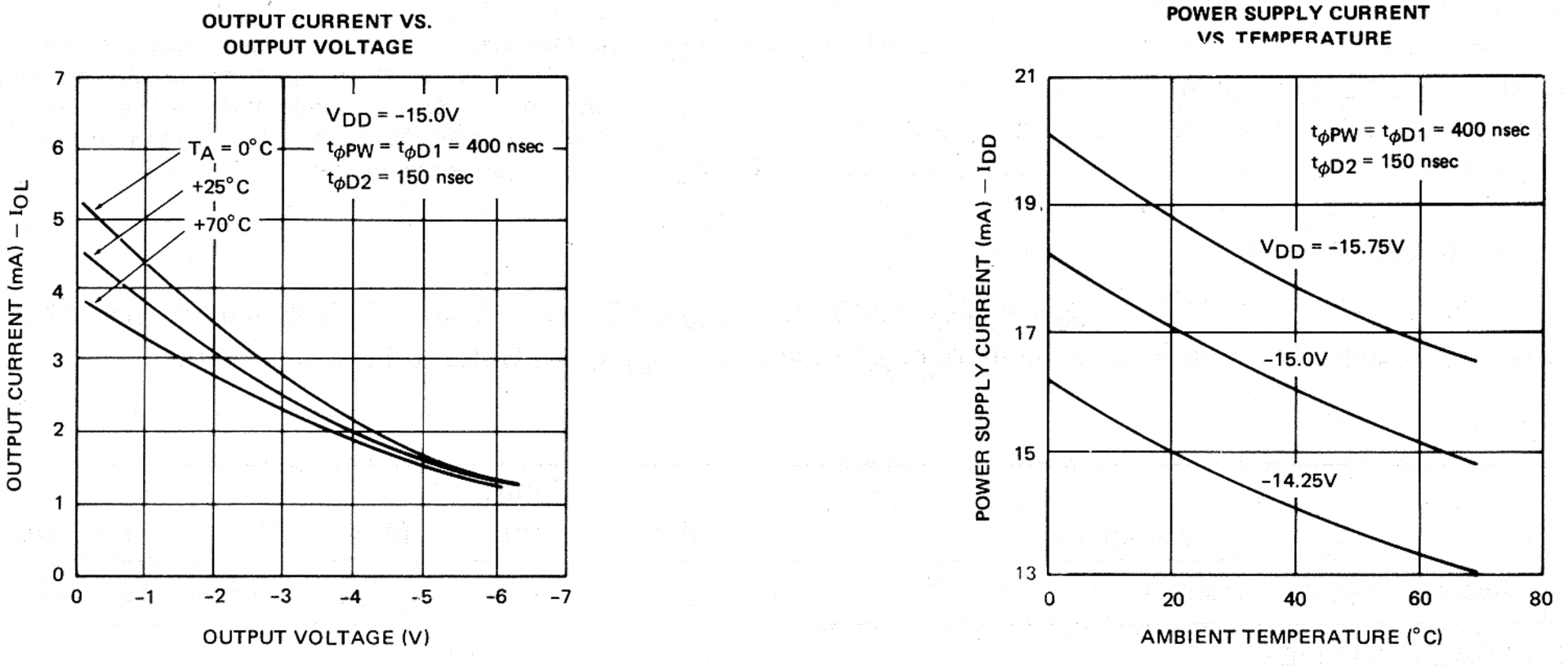
Typical D.C. Characteristics
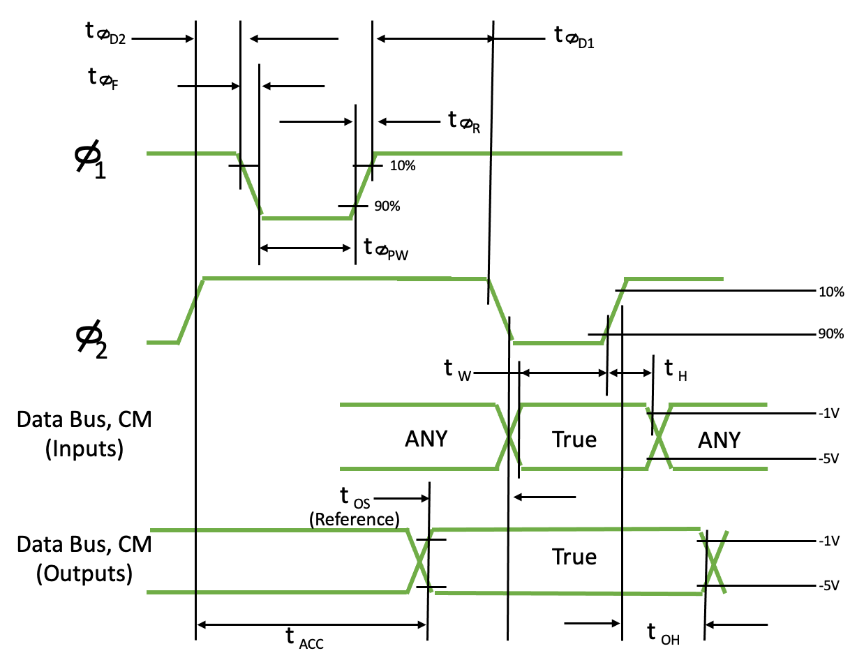
A.C. Characteristics
\(T_{A}\) = \(0^{o}\) C to \(70^{o}\) C
\(V_{SS}\) - \(D_{DD}\) = 15V ± 5%
Symbol |
Parameter |
Min |
Limit Typical |
Max |
Unit |
Test Conditions |
|---|---|---|---|---|---|---|
\(t_{CY}\) |
Clock Period |
1.35 |
2.0 |
\({\mu}sec\) |
||
\(t_{\phi R}\) |
Clock Rise Times |
50 |
ns |
|||
\(t_{\phi F}\) |
Clock Fall Times |
50 |
ns |
|||
\(t_{\phi PW}\) |
Clock Width |
380 |
480 |
ns |
||
\(t_{\phi D1}\) |
Clock Delay \(t_{\phi 1}\) to \(t_{\phi 2}\) |
400 |
550 |
ns |
||
\(t_{\phi D2}\) |
Clock Delay \(t_{\phi 2}\) to \(t_{\phi 1}\) |
150 |
ns |
|||
\(t_{W}\) |
Data-In, CM, SYNC Write Time |
350 |
100 |
ns |
||
\(t_{H}\) [1,3] |
Data-In, CM, SYNC Hold Time |
40 |
20 |
ns |
||
\(t_{OS}\) [2] |
Set Time (Reference) |
0 |
ns |
|||
\(t_{ACC}\) |
Data-Out Access Time |
|
ns |
\(C_{OUT}\) = |
||
\(t_{OH}\) |
Data-Out Hold Time |
50 |
150 |
ns |
\(C_{OUT}\) = 20pF |
|
\(t_{D}\) |
I/O Output Delay |
1500 |
ns |
\(C_{OUT}\) = 100pF |
Note
[1] \(t_{H}\) measured with \(t_{\phi R}\) = 10nsec
[2] \(T_{ACC}\) is Data Bus, SYNC and CM-line output access time referred to the \({\phi}_{2}\) trailing edge which clocks these lines out. \(t_{OS}\) is the same output access time referred to the leading edge of the next \({\phi}_{2}\) clock pulse.
[3] All MCS-40 components which may transmit instruction or data to the 4004 at \(M_{2}\) and \(X_{2}\) always enter a float state until the 4004 takes over the data bus at \(X_{1}\) and \(X_{3}\) time. Therefore, the \(T_{H}\) requirement is always insured since each component contributes \(10{\mu}A\) of leakage current and 10pF of capacitance, which guarantees that the data bus cannot change faster than \(1V/{\mu}sec\)
4002 Timing Diagram
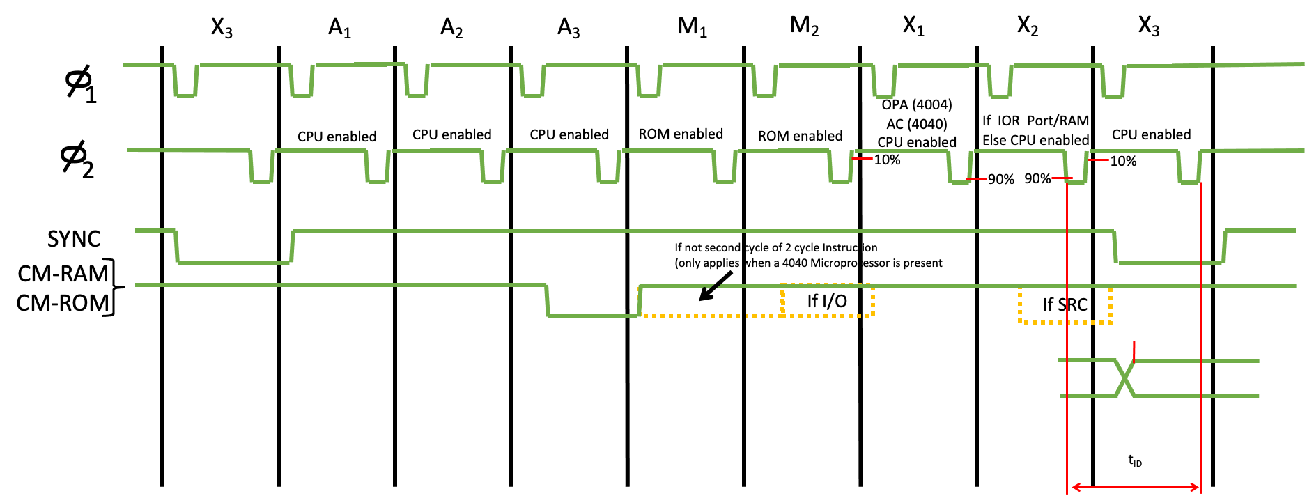
4002 Timing Diagram Detail