Intel 4004 Chip History
In 1969 Busicom contracted Intel to design a set of chips to be used in a new high perfomance calculator. Ted Hoff, Federico Faggin and Stan Mazor came up with a design that involved four different chips. The CPU was eventually to be called a microprocessor.
Later Intel negotiated for a return of the rights for the chips, which had gone to Busicom in the original contract.
The 4000 Family (A.K.A. Busicom Chip Set / MCS-4 Chip Set)
The 4000 family consisted of four different chips:
a 2048-bit ROM with a 4-bit programmable input-output port (4001)
a 4-registers x 20-locations x 4-bit RAM data memory with a 4-bit output port (4002)
an input-output expansion chip, consisting of a static shift register with serial input and serial and parallel output (4003)
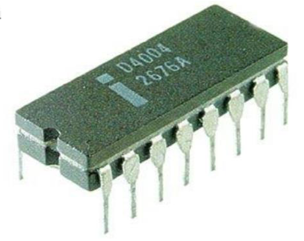
a 4-bit CPU chip (4004)
Other chips in the 4xxx family were:
an 8-bit address latch for access to standard memory chips, and one built-in 4-bit chip select and I/O port (4008)
a program and I/O access converter to standard memory and I/O chips (4009)
an 8192-bit( 1024 × 8) ROM w/ 4-bit I/O Ports (4208)
a general purpose Bye I/O port (4211))
a keyboard/display interface (4269)
a memory interface (combined functions of 4008 and 4009)(4289)
an 8k mask-programming ROM (4308)
a 16384-bit (2048 × 8) Static ROM (4316)
a 2048-bit (256 × 8) EPROM (4702)
a 5.185 MHz Clock Generator Crystal for 4004/4201A or 4040/4201A (4801)
All the chips were packaged in 16-pin, dual-in-line packages. This package restriction was imposed by Intel’s management, who at the time considered any package with more that 16 pins uneconomical, despite the fact that 40-pin packages were widely used by other semiconductor companies.
This unfortunate choice considerably constrained the performance of the system.
Address and data had to be multiplexed onto the pins (one of the claims of
Patent number US3821785), causing a major
penalty in the instruction cycle execution.
The instruction cycle of 10.8 microseconds could have been easily reduced to 4 microseconds by a more appropriate package choice.
The 4000-family was completed by March 1971, in production by June 1971 and introduced to the general market in November 1971 with the name MCS-4.
MCS-4
The MCS-4 is a microprogrammable computer set designed for applications such as test systems, peripherals, terminals, billing machines, measuring machines, numeric and process control.
The 4004 CPU, 4003 Shift Register, and 4002 RAM are standard building blocks. The 4001 ROM contains the custom microprogram and is implemented as a metal mask according to customer specifications.
MCS-4 systems readily interface to switches, keyboards, displays, teletypewriters, printers, readers, A-D converters and other popular peripherals.
A system built with the MCS-4 micro computer set can have up to 4k * 8-bit ROM words, 8192 * 4-bit RAM characters, and 128 I/O lines without requiring any interface logic. By adding a few gates, the MCS-4 can have up to 48 RAM and ROM packages in any combination, and 192 I/O lines. The minimum configuration consists of one CPU and one 256 * 8-bit ROM.
The MCS-4 has a very powerful instruction set that allows both binary and decimal arithmetic. It includes conditional branching, jump to subroutine, and provides for the efficient use of ROM look-up tables by indirect fetching.
The Intel MCS-4 micro computer set (4001/2/3/4) is fabricated with Silicon Gate Technology . This low threshold technology allows the design and production of higher performance MOS circuits and provides a higher functional density on a monolithic chip than conventional MOS technologies.
Busicom 141-PF
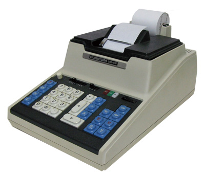
In the case of the Busicom 141-PF (also marketed as the NCR-18-36), the ROM contained the custom microprogramming to allow the MCS-4 chipset to operate as a calculator.
