The Intel 4004 Chip
The Intel 4004 chip was introduced in 1971 as part of the Intel 4000 family; 4-bit central processing unit (CPU), fabricated with P-channel silicon gate MOS technology.
The 4004 was designed to be used with other members of the MCS-4/40 family (4001, 4002, 4003).
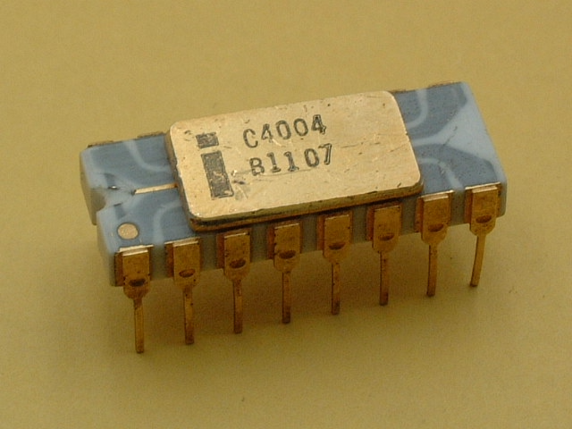
The packaging of the Intel 4004 (and the Second Source manufacturers) is shown below:
Manufacturer |
Model |
Package |
|---|---|---|
Manufacturer |
Model |
Package |
Intel |
C4004 |
16-pin Ceramic DIP |
Intel |
D4004 |
16-pin Ceramic DIP |
Intel |
P4004 |
16-pin Plastic DIP |
National Semiconductor |
INS4004D |
16-pin Ceramic DIP |
National Semiconductor |
INS4004J |
16-pin side-brazed Ceramic DIP |
Hitachi |
HD35404 |
16-pin DIP |
Microsystems International |
MF7114 |
Internally, the 4004 is a 4-bit microprocessor with 8-bit instructions. It is clocked at a frequency of 500KHz - 740KHz. It contains 4096x8-bit ROM and 1280x4-bit RAM, with 2,300 transistors at a 10 micron definition. There are 45 instructions (46 including NOP) with a 4 level stack and sixteen 4-bit (or eight 8-bit) registers
For more detail, see the hardware characteristics or the instruction format.
Logically, the Intel 4004 is set out as shown:
Internal
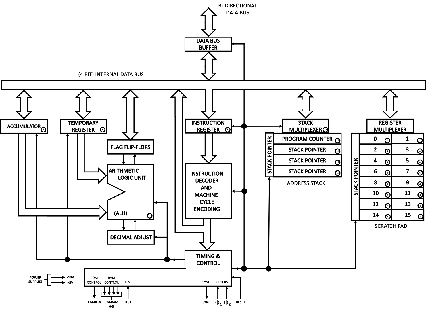
including external
The circled numbers relate to the pins as shown below:
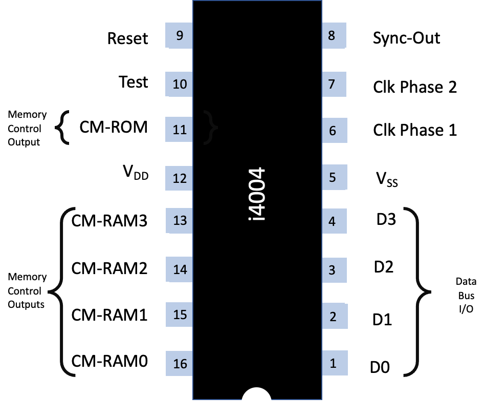
Pins described as follows:
Pin(s) |
Description |
|---|---|
D0 - D3 |
Bi-Directional Data Bus. |
V SS |
Most positive voltage |
Clk-Phase 1 |
2 phase clock inputs |
SYNC |
SYNC Output. |
RESET |
RESET input. |
TEST |
TEST input. |
CM-ROM |
CM-ROM Output. |
V DD |
V DD - 15 +/-5% main supply voltage |
CM-RAM0 - |
CM-RAM Output. |
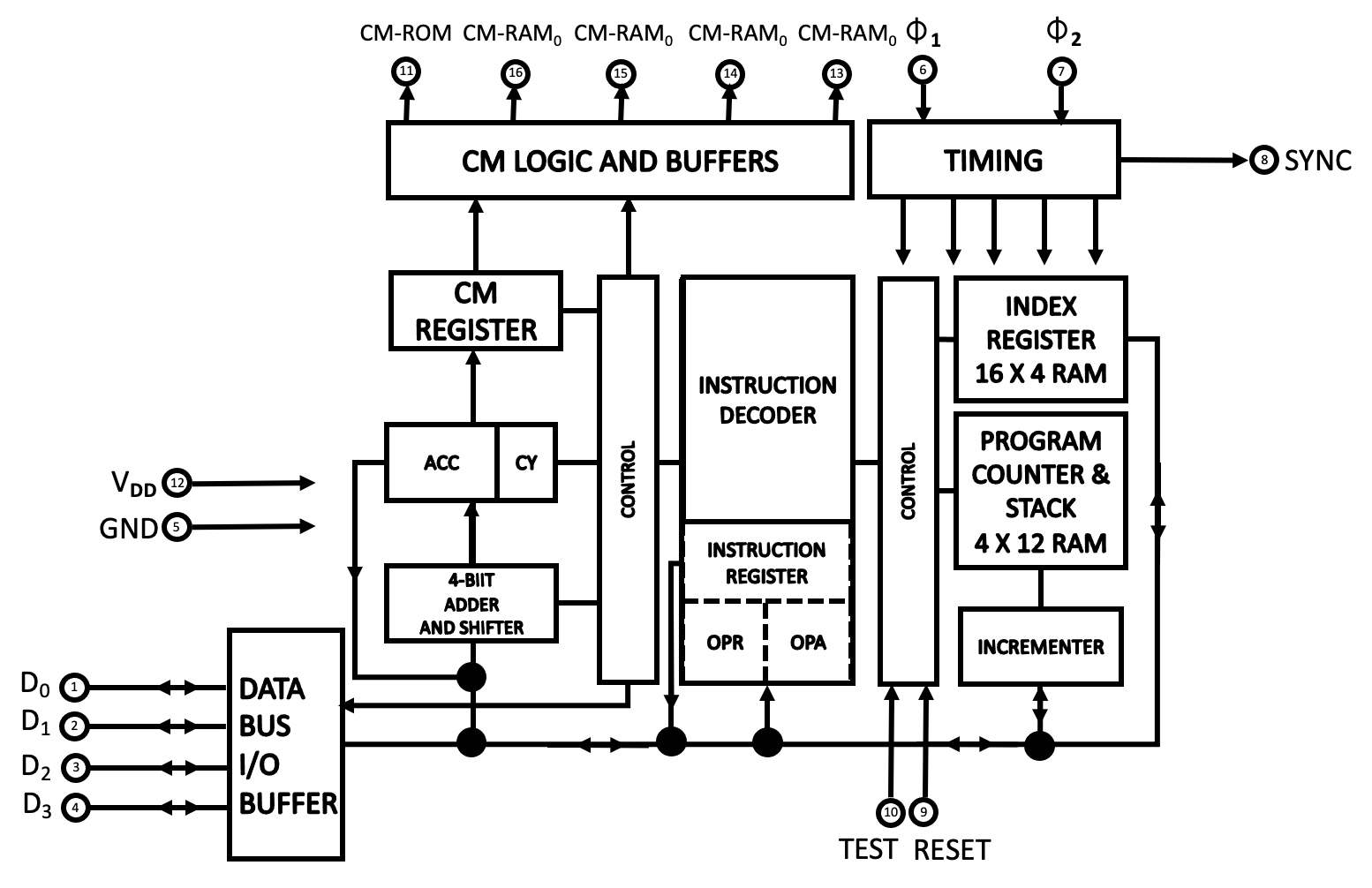
The CPU consists of the following components:
Component |
|
|---|---|
a |
4-bit adder |
b |
64-bit (16 x 4) index register |
c |
48-bit Program Counter |
d |
Stack (nesting up to 3 levels if possible) |
e |
Address incrementer |
f |
8-bit instruction register and decoder |
g |
Control logic |
Information flows between the 4004 and the other chips through a 4-line data bus. One 4004 may be combined with up to 48 ROM (4001) and RAM (4002) chips in any combination.
A typical machine cycle starts with the CPU sending a synchronisation signal (SYNC) to the ROMs and RAMs. Next, 12 bits of ROM address are sent to the data bus using three clock cycles (@ 0.75Mhz). The address is then incremented by one and stored in the Program Counter.
The selected ROM sends back 8 bits of instruction or data during the following two clock cycles.
This information is stored in two registers: OPR and OPA. The next three clock cycles are used to execute the instruction. (See Basic Instruction Cycle on Page 5.)
The ROM bank is controlled by a command ROM control signal (CM-ROM) and up to four RAM banks are controlled by four RAM control signals (CM-RAM 0, CM-RAM 1, CM-RAM 2, CM-RAM 3)
Bank switching is accomplished by the execution of a “DCL” instruction.
An input test signal (TEST) is used in conjunction with the jump on condition (”JCN”) instruction. An external RESET signal is used to clear all registers and flip-flops. To fully clear all registers, the RESET signal must be applied for at least 8 memory cycles (8 x 8 clock periods). After RESET the program will start from “0” step and CM-RAM 0 will be selected.
The instruction repertoire of the 4004 consists of :
Instruction Type |
Number |
|---|---|
Machine instructions (5 of which are double length) |
16 |
Accumulator group instructions |
14 |
Input/output and RAM instructions |
16 |
Total |
45 |
No-Operation |
1 |
TOTAL |
46 |
Note
Bank Switching
Bank switching is accomplished by the CPU after receiving a “DCL” (designate command line) instruction.
Prior to the execution of the DCL instruction the desired CM-RAM i code has been stored in the accumulator (for example,
through an LDM instruction).
During DCL the CM-RAM i code is transferred from the accumulator to the CM-RAM register.
The RAM bank is then selected starting with the next instruction.
