DCL
Name |
Designate Command Line |
Function |
Select a RAM bank |
Syntax |
DCL |
Assembled |
|
Binary |
11111101 |
Decimal |
253 |
Hexadecimal |
0xFD |
Symbolic |
|
Execution |
1 word, 8-bit code and an execution time of 10.3 \({\mu}\) sec |
Side-effects |
Not Applicable |
Implemented |
Detailed Description
The content of the three least significant accumulator bits is transferred to the comand control register within the CPU. This instruction provides RAM bank selection when multiple RAM banks are used, since there could be up to 8 RAM banks.
(If no DCL instruction is sent out, RAM Bank number zero is automatically selected after application of at least one RESET).
DCL remains latched until it is changed.
The opcode for this instruction does not contain any additional data:

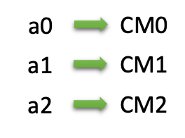
The least significant 3 bits of the accumulator determine which RAM bank is selected (detailled in the table below, along with the bits of the command register).
Accumulator |
CM-RAM i |
RAM |
|||
|---|---|---|---|---|---|
0x000 |
CM-RAM 0 |
0 |
|||
0x001 |
CM-RAM 1 |
1 |
|||
0x010 |
CM-RAM 2 |
2 |
|||
0x100 |
CM-RAM 3 |
3 |
|||
0x011 |
CM-RAM 1 |
CM-RAM 2 |
4 |
||
0x101 |
CM-RAM 1 |
CM-RAM 3 |
5 |
||
0x110 |
CM-RAM 2 |
CM-RAM 3 |
6 |
||
0x111 |
CM-RAM 1 |
CM-RAM 2 |
CM-RAM 3 |
7 |
