4003 Hardware Characteristics
Absolute Maximum Ratings
Ambient Temperature Under Bias |
0 o C to +70 o C |
Storage Temperature |
-55 o C to +125 o C |
Input Voltage and Supply Voltage |
+0.5 to -20 V |
Power Dissipation |
1.0 W |
Note that stresses above those listed in “Absolute Maximum Ratings” may cause permanent damage to the device. This is a stress rating only and functional operation of the device at these or any other conditions above those indicated in the operational sections of this specification is not implied.
D.C. and Operating Characteristics
\(T_{A}\) = \(0^{o}\) C to \(70^{o}\) C
\(V_{SS}\) - \(D_{DD}\) = 15V ± 5%
\(t_{\phi PW}\) = \(t_{\phi D1}\) = 400nsec
\(t_{\phi D2}\) = 400nsec ; unless otherwise specified.
logic “0” is defined as the more positive voltage (\(V_{IH}\), \(V_{OH}\))
logic “1” is defined as the more negative voltage (\(V_{IL}\), \(V_{OL}\))
SUPPLY Current
Symbol |
Parameter |
Min |
Limit Typical [1] |
Max |
Unit |
Test Conditions |
|---|---|---|---|---|---|---|
\(I_{DD}\) |
Average Supply Current |
5.0 |
8.5 |
mA |
\(T_{WL}\) = \(T_{WH}\) = \(8{\mu}s\) ; |
|
Input Characteristics |
||||||
\(I_{LI}\) |
Input Leakage Current |
10 |
\({\mu}A\) |
\(V_{IL}\) - \(V_{DD}\) |
||
\(V_{IH}\) |
Input High Voltage |
\(V_{SS}\) -1.5 |
\(V_{SS}\) +0.3 |
|||
\(V_{IL}\) |
Input Low Voltage |
\(V_{DD}\) |
\(V_{SS}\) -4.2 |
V |
||
I/O Output Characteristics |
||||||
\(I_{OH}\) |
Parallel Out Pins |
0.6 |
1.0 |
\({\mu}A\) |
\(I_{OUT}\) = 0 |
|
\(I_{OL}\) |
Serial Out Pins Sinking Current, “1” Level |
1.0 |
2.0 |
\({\mu}A\) |
\(V_{OUT}\) - \(V_{SS}\) - 0.5V |
|
\(V_{OL}\) |
I/O Output Low Voltage |
\(V_{SS}\) -11 |
\(V_{SS}\) -7.5 |
\(V_{SS}\) -6.5 |
V |
\(I_{OUT}\) = \(50{\mu}A\) |
\(R_{OH}\) |
Parallel Out Pins |
400 |
750 |
\(k{\Omega}\) |
\(I_{OUT}\) = 0 |
|
\(R_{OH}\) |
Serial Out Resistance, “0” Level |
650 |
1200 |
\(k{\Omega}\) |
\(V_{OUT}\) - \(V_{SS}\) - 0.5V |
|
Capacitance
f = 1MHz; \(V_{IN}\) = 0V; \(T_{A}\) = \(25^{o}C\) Unmeasured Pins Grounded
Symbol |
Test |
Typ. |
Max |
Unit |
|---|---|---|---|---|
\(C_{IN}\) |
Input Capacitance |
5 |
10 |
pF |
Note
[1] Typical values are to \(T_{A}\) = \(25^{o}\) C and Nominal Supply Voltages
[2] For Transistor-transistor logic (TTL) compatibility, use \(12 k{\Omega}\) external resistor to \(V_{DD}\)
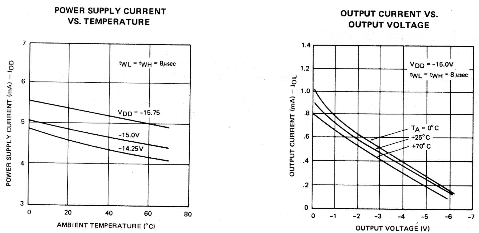
Typical D.C. Characteristics
A.C. Characteristics
\(T_{A}\) = \(0^{o}\) C to \(70^{o}\) C
\(V_{DD}\) = 15V ± 5%
\(V_{SS}\) = GND
Symbol |
Parameter |
Min |
Limit Typical |
Max |
Unit |
Test Conditions |
|---|---|---|---|---|---|---|
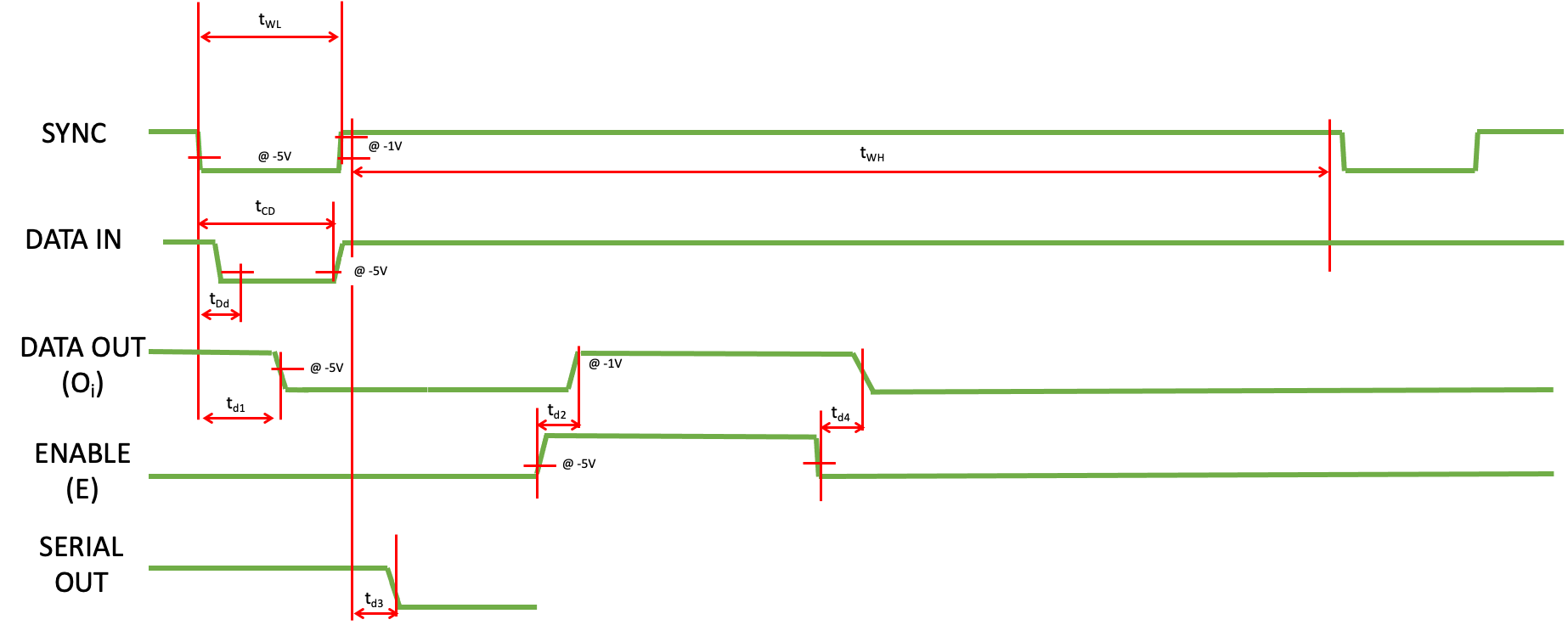
\(t_{WL}\) |
CP Low Width |
6 |
10,000 |
\({\mu}sec\) |
||
\(t_{WH}\) [1] |
CP High Width |
6 |
\({\mu}sec\) |
|||
\(t_{CD}\) |
Clock-On to Clock-Off Time |
3 |
\({\mu}sec\) |
|||
\(t_{Dd}\)[2] |
CP to Data Set Delay |
250 |
ns |
|||
\(t_{d1}\) |
CP to Data Out Delay |
250 |
1750 |
ns |
||
\(t_{d2}\) |
Enable to Data Out Delay |
350 |
ns |
\(C_{OUT}\) = 20pF |
||
\(t_{d3}\) |
CP to Serial Out Delay |
200 |
1250 |
ns |
\(C_{OUT}\) = 20pF |
|
\(t_{d4}\) |
Enable to Data Out Delay |
40 |
1.0 |
\({\mu}sec\) |
\(C_{OUT}\) = 20pF |
Note
[1] \(t_{WH}\) can be any time greater than \(6{\mu}s\)
[2] Data can occur prior to CP
4003 Timing Diagram